Rigid PCB – Process & Control Point
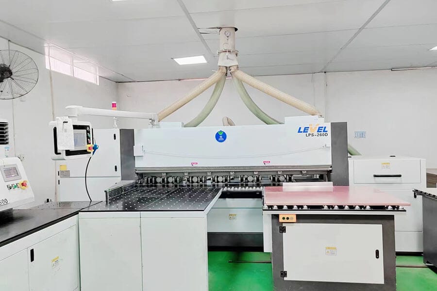
LAMINATE SHEAR
Auto material cutting machine, cut sheet size 37*49inch, 41*49inch, 43*49inch to working PNL size.
Check point:
- Base Material Type
- Dimension
- No Dent、No Scratch
- Quantity
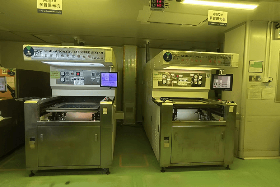
INNERLAYER IMAGE
Laser direct imaging
Check point:
1.Correct CAM data
Auto exposure machine
Check point:
1.Energy
2.Vacuity
3.Environment
Develop
check point:
1.Temperature
2.Pressure
3.Concentration
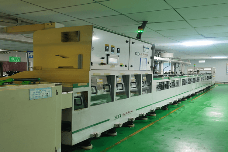

INNERLAYER ETCHING
After development, the non-product copper is etched away.
Check point:
1.Temperature
2.Speed、Pressure
3.Concentration
4.Line width/space
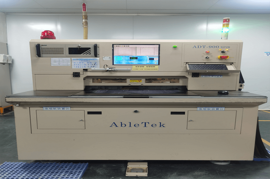
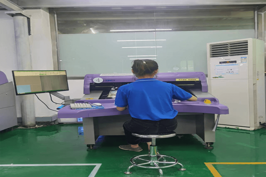
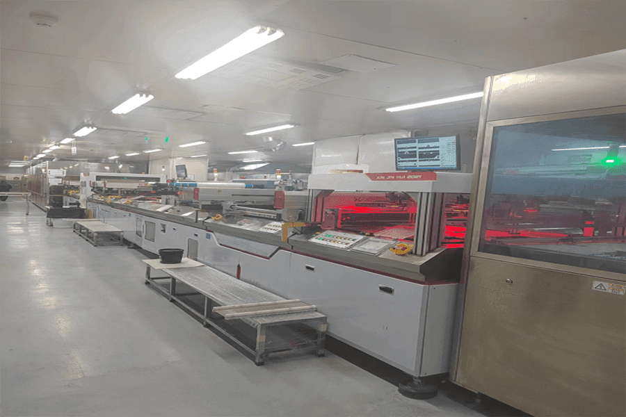
AOI INSPECTION
AOI(Automatic Optic Inspection)
Check point:
1.Open/short
2.Copper Residue


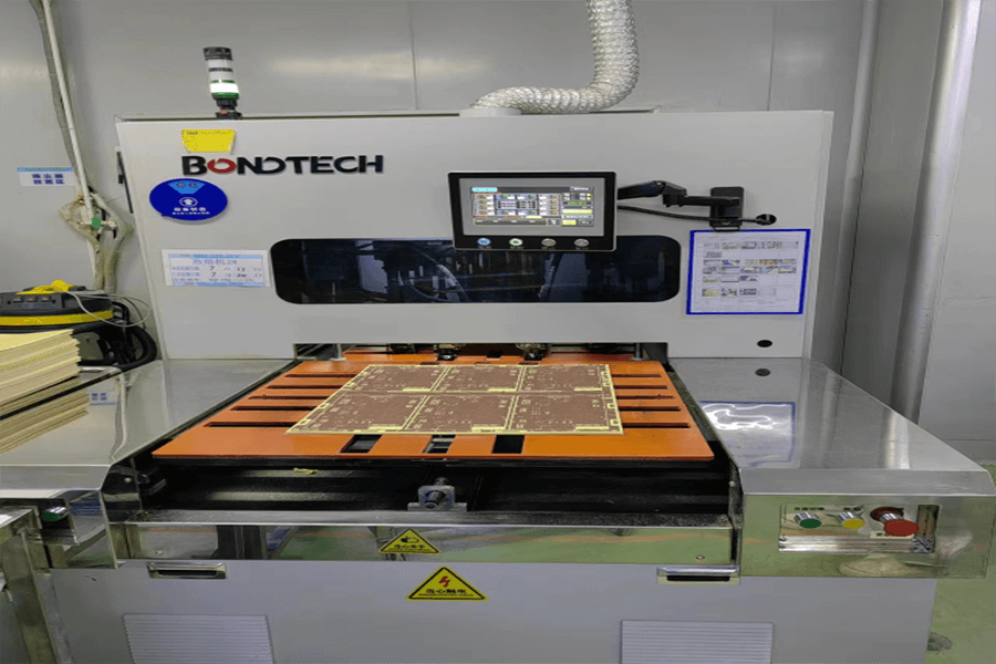

LAMINATION
Horizontal black oxidation
Check point: 1.Concentration 2.Temperature 3.Coating Thinkness
Vertical black oxidation
Check point: 1.Concentration 2.Etching Rate 3.Temperature
Vacuum high-presure laminated machine
Check point: 1.Temperature 2.Temp. increase Rate 3. Pressure
Quality check point: 1.Board Thinkness 2.Delamination 3.Appearance
DRILLING
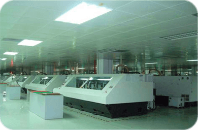
Mechanical drilling
Check point:
1.Hole Size
2.Hole Wall Roughness
3.Registration
4.The amount of holes
5.Appearance
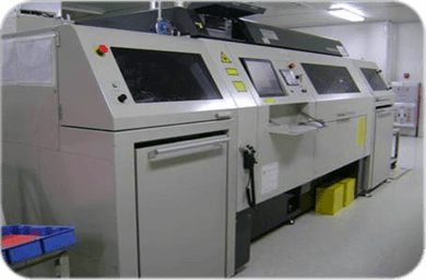
Laser drilling, drill micro via holes
Check point:
1.Laser drill completely
2.Hole diameter
3.Hole shape
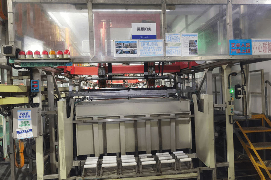
PTH
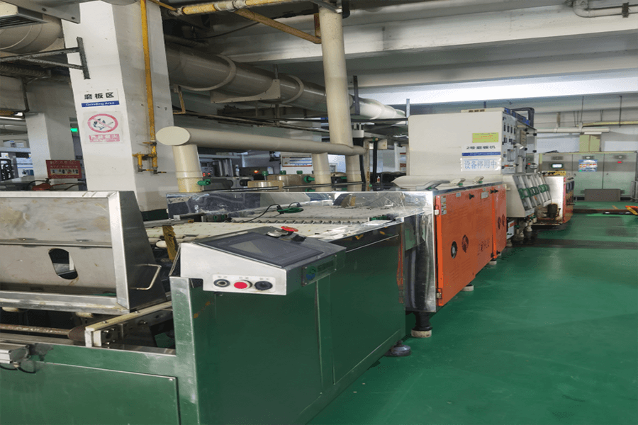
Check point:
1. Desmear parameters
2.Deposition rate
3.Electricity
4.Temperature
5.Microetch rate
6.Back Light Test
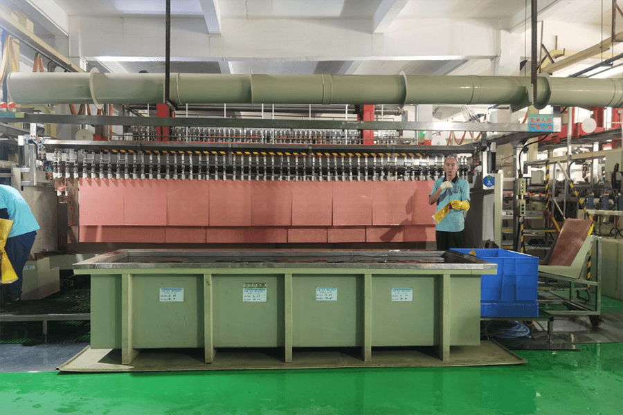
PANEL PLATING
Horizontal plating
Check point:
1.Temperature
2.Concentration
3.Current Density
Vertical plating
Check point:
1.Temperature
2.Concentration
3.Current Density


EXTERNAL LAYER IMAGE
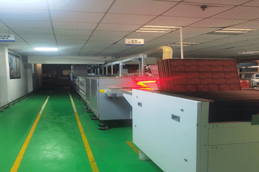
laser direct imaging
Check point:
1.Correct CAM data
Auto exposure machine
Check point:
1.Energy
2.Vacuity
3.Environment
PATTERN PLATING
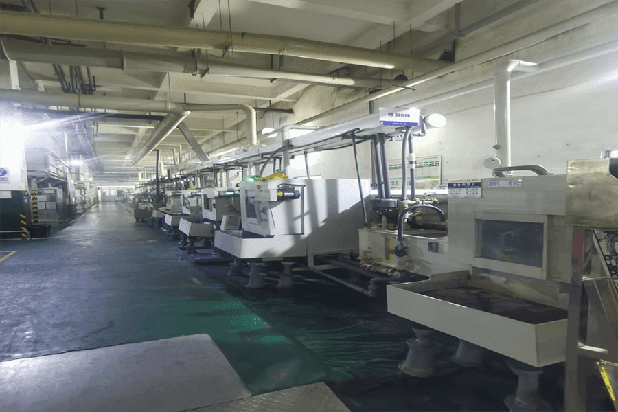
Pattern plating
Check point:
1.Temperature
2.Concentration
3.Current Density
4.Check scratching the tin on the lines
Quality check point:
1.Hole Wall thickness.
2.Surface copper thickness

EXTERNAL LAYER ETCHING
Check point:
1.Temperature
2.Etching speed
3.Pressure
3.Concentration
4.Width/space
AOI INSPECTION
AOI(Automatic Optic Inspection)
Check point:
1.Open/short
2.Copper Residue
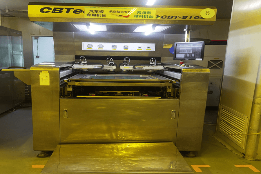
SOLDER MASK
Check point:
1.No Exposure copper
2.No Mask on Pad
3.No Scratch
4.The thickness of solder mask.
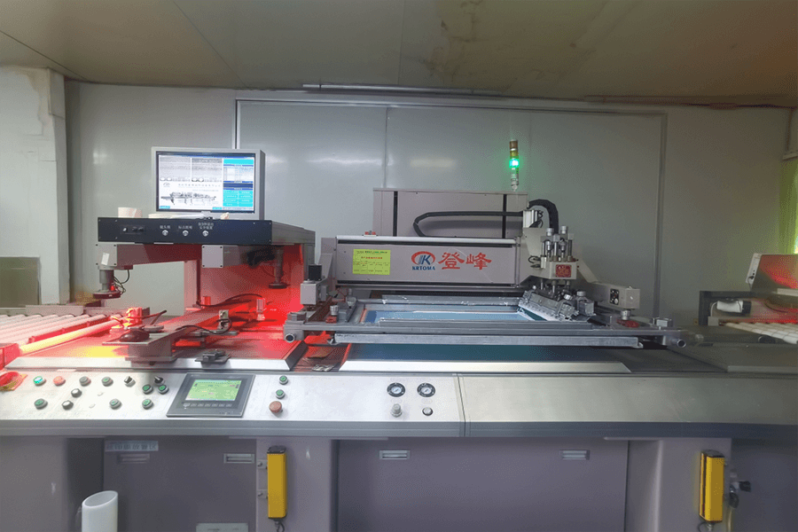
SILKSCREEN
Auto-printing
Check point:
1.correct CAM data
2.Registration
3.Definition
4.No scratching

Immersion gold
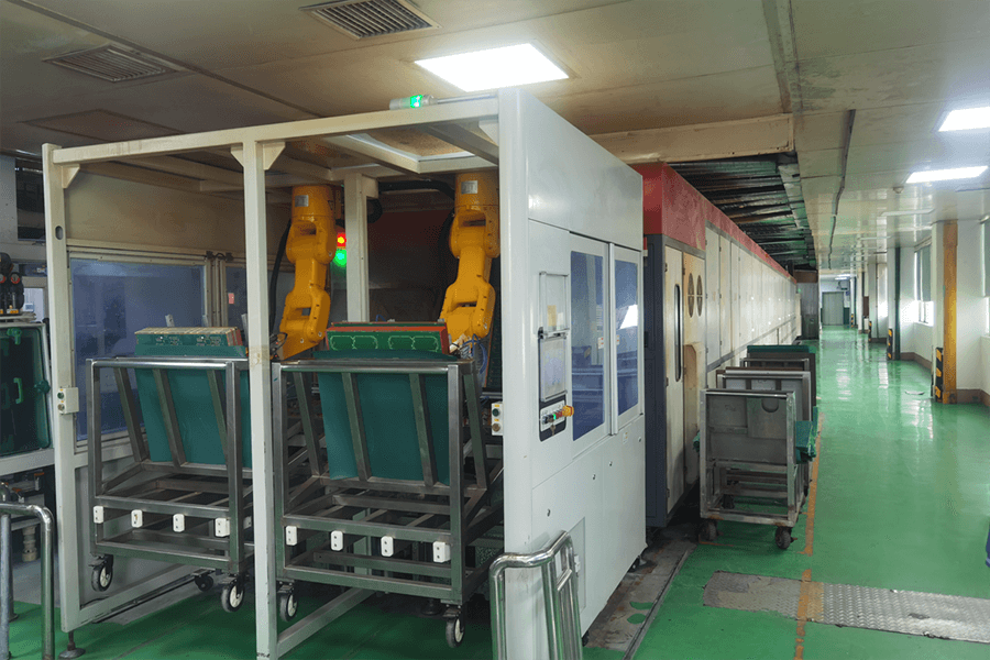
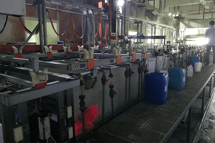
Immersion Gold
Check point:
1.Temperature
2.Concentration
Quality check point:
1.Au / Ni thickness
2.Phosphorus percent
3.Apperance
Hot air leveling
Check point:
1.Angle of Air Knives
2.Solder Bath Temp.
3.Air Knives Temp.
Quality check point:
1.Sn/Pb Thinkness
2.Apperance
FINAL SHAPING
CNC routing for finish board size
Check point:
1.Dimension
2.No Powder Residue
3.No Scratch

ELECTRICAL TEST
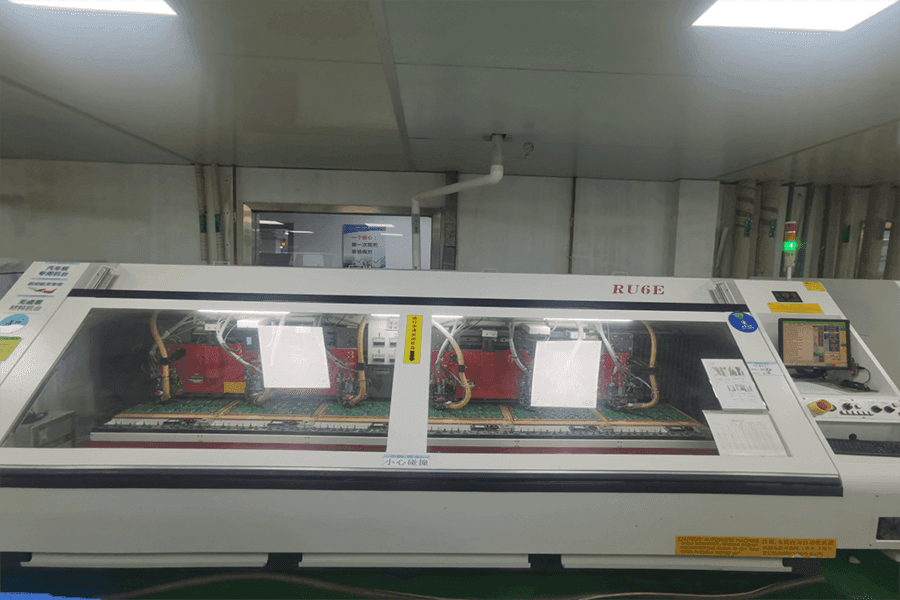
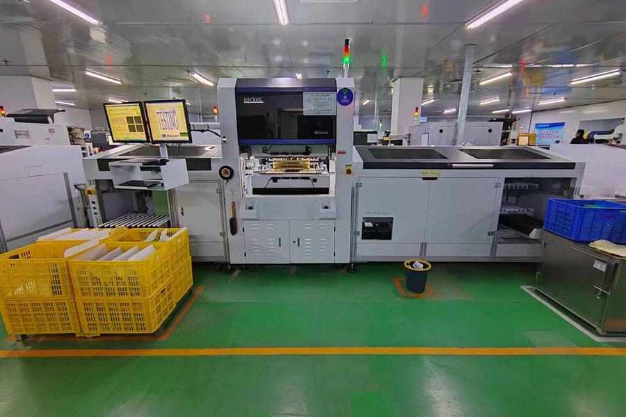
Flying probe tester
Check point:
1.Open
2.Short
3.Circumferential Separation
FQC
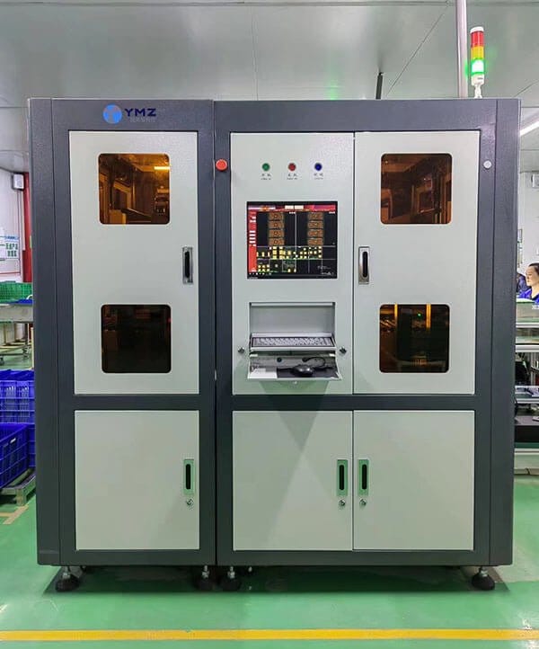
Final quality control, visual inspection
Check point:
1.Visual performance of solder mask, holes, traces…
2.V-cut routing, drilling
3.The quality of surface treatment.
4.Warp and twist
FQA
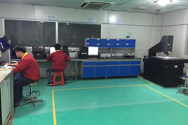
Check point:
1. Cross section
2. Dimension
3. Solderability test
4. Thermal stress test
5. Iron contamination test
6. Thickness of surface treatment
7. Preparing the relevant reports

OUR PARTNERS



HOW AUSPI HELP YOU ?
With over 20 years of experience, Auspi has firmly established itself as a leader in client satisfaction across diverse industries. Our strategically positioned facilities in the Americas, Europe, and Asia allow us to effectively meet both your geographical and cost requirements. We carefully balance quality and affordability, ensuring that every penny you invest delivers exceptional value.
In the fast-evolving and competitive electronics industry, we remain agile and innovative. By continuously expanding our service offerings, we ensure that we not only meet but exceed the expectations of our valued partners. Your success is our priority, and we are dedicated to staying at the cutting edge of industry advancements to support your growth.


01/ Reliability
- Full Compliance with NDA Requirement;
- Strictly Follow Customer’s Original Design;
- Good Quality Performance & Keep Improving;
- Honoring Our Commitments

02/ Expertise
- Full Manufacturing Process Coverage;
- Decades Focusing & Rich Experience;
- Turn Key & One-Stop Solution
- Components Sourcing & SCM

03/ Fast Response
- 8 hours RFQ Reply & Online Chat
- 24 Hours Feedback on Customer Complain
- 72 Hours PCB Bear Board Sampling;
- 2-3 Weeks PCBA Prototyping (TurnKey BoM)

04/ Flexibility & Quickturn
- NO Minimum Order(MoQ) Requirement;
- Wide Rage of Components Inventory;
- Expedite Services;
- Diversity, Equity & Inclusion

05/ Worldwide Supply
- 8 Branches Worldwide; (see contact us)
- 4 Manufacturing Bases Located in China, Czech Republic, Mexico & Malaysia;
- Multi-sites Phone Access & Local Supporting

06/ Reasonable Cost
- Transparent, BoM Cost Breakdown;
- Live Stock and Pricing Data;
- Alternative Scenarios Proposal
- Competitive Pricing

