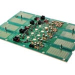
A printed circuit board (PCB), also called printed wiring board (PWB) is a medium used in electronic engineering to connect electronic components to one another. Typically, the copper wiring on the PCB is designed and analyzed using a diagram, called a schematic, and the schematic consists of electronic component symbols connected by lines. After the copper wires are printed on the board following a successful schematic, the components should be able to communicate in a controlled manner once assembled onto the board.
Simply put, a PCB is just a printed copper wire layout that is ready to have physical and electrical connection with components. And the process of connecting designated electronic components to the bare PCB is called printed circuit board assembly (PCBA). Here in this article, let’s focus on the PCB!
The Structure of a PCB
Typically, a very basic PCB is a flat, rigid, insulating material with thin conductive copper layers covered on the surface of both sides. During the manufacturing process, most of the copper on the surface will be etched away leaving only the designed schematic on the surface. That is a circuit “printed” on the board. After that, for the multilayer boards, in order for different layers to have physical and electrical connections pads and vias of different sizes and kinds will have to be drilled. Depending on the layer counts of the board, this process can repeat many times.
A standard multilayer PCB consists of cores, copper layers, prepreg and solder masks on the top of both sides, while core is the fiberglass that gives the board the stiffness, and prepreg is the adhesive that binds the layers together. The most commonly used core is FR-4 which functions well as an electrical insulator, and it has a good strength-to-weight ratio while being flame resistant. On the surface layers, there is a layer of solder mask on each side of the board covering the coppers to prevent oxidation.
Reasons for using multiple layers in a PCB
- Reduced complexity
Multiple layers make it easy for the PCB traces to route by jumping over from one layer to another to complete the path. Hence many complex circuits can be routed easily. - Miniaturization
Reducing the size of PCB saves a lot of resources right from PCB board up to packaging materials. Also, the demand for compact electronic devices boosts the need for miniaturized circuits. - Supply and ground isolation
In PCBs with 4 or more layers, supply and ground is provided with 1 layer each. This provides isolation between supply and ground pins and hence avoids short circuit.
To design a PCB
PCB designing can be a very complicated and technical work since designers have to understand all the electrical parameters and have a deep understanding to the functions of different types of electronic components while being familiar with the design rules and requirements of PCB manufacturing.
Regardless of the complexity and function of the circuits, designers have to abide by a few responsibilities:
- Design Schematics
- Select Components conforming to Design Standards
- Analyze mathematically through simulation
- Prototyping and testing the circuit
- Proving the circuit works for production!!!


