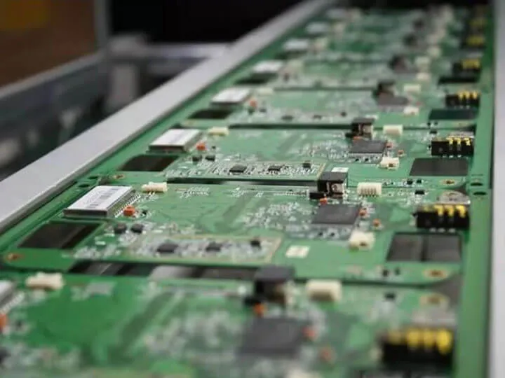
PCBA (Printed Circuit Board Assembly), namely electronics assembly is a process of attaching electronic components onto the PCB (Printed Circuit Board). When you look at a PCB, have you ever how the chips and other components are solidly stuck onto the board? That is what needs to be accomplished during the process of PCBA. Not only are the components physically stuck on the board, but the electrical connection between the board and the electronics components is built during the PCBA process.
PCBA Process
- Solder Paste Stenciling
After a bare PCB is fabricated, pads are left with no soldier mask covered for the SMT (Surface Mount Technology).
The Solder Paste will be applied on the pads during this process before the electronic components sit on them. The paste composes of 96.5% tin, 3% silver and 0.5% copper. They will, later on, facilitate the physical and electrical connections between the devices/components and the board.
A professional Solder Paste Stencilling machine can hold the PCB and apply a precise amount of paste on the intended areas. As the machine spreads the paste across the stencil, the paste will be applied evenly onto the pads. The solder paste stencil is a sheet of metal like stainless steel or nickel that has holes cut very accurately according to the solder paste layer of the PCB layout design.
- Pick and Place
After the solder paste is applied, the PCB goes to a pick-and-place machine. A robotic device places SMDs on the board at a very fast pace. They are preprogrammed for each project so that they know where to place the components.
Nowadays, the components are getting smaller and smaller. Pick and place machines will have capacity on the smallest component they can pick up. If your components are too small, you might require a special machine for the pick and place process.
- Reflow Soldering
Once the solder pastes and SMDs are all in place, there comes a reflow soldering process. As the paste solidifies, the SMDs are held tightly on the board.
This process is done in a reflow oven with a series of heaters gradually heating the board to 250 degrees Celsius. Then, the solder paste is properly melted. After that, the PCB continues to move through the oven and cools down gradually. Then, the paste is cooled and solidified in a controlled manner.
- Inspection and Quality Control
Once the SMT process is done, there will be an inspection examining the physical and electrical connections between the devices and the board. Bad solder joints often result in serious quality problems.
Automatic Optical Inspection (AOI) is a common inspection for large batches of PCBAs. An AOI machine has a series of cameras to examine PCBs. The cameras are arranged at different angles to view solder connections. As different quality solder connections reflect the light differently, the AOI machine can recognize bad solders.
The malfunctioning boards will be sent back to be cleared and reworked or wasted depending on the standard requirement.
- Through-Hole Component Insertion
Aside from the pads, Plated Through-Holes (PTH) are also left on the PCB for the through-Hole Component Insertion process when a PCB requires PTH components. A PTH is a hole plated through the board. PTH components can pass signals from one side to the other.
The process of PTH components assembly requires more manpower since the components have to be inserted onto the board manually. Usually, in the PTH component insertion line, one worker is only inserting one component, and then the board gets passed to another worker to insert another component. This goes on until all the components are inserted into the board.
- Wave Soldering
A wave solder machine consists of a flux applicator, a pre-heat tunnel and a solder pot with a pump. The machine is good for mass production as it eliminates hand soldering, leading to faster production and higher quality.
Once all the PTH components are in place, the boards are loaded onto the conveyer of a wave solder machine. First, the flux is applied to the joints on the bottom of the circuit board. Then, the boards travel through a heat tunnel to pre-heat the board and activate the flux. As the boards leave the heat tunnel, the wave pump starts, and the conveyer continues carrying the boards exposing them to the wave of molten solder beneath. As the board skims along the edge of the solder wave, all the joints exposed to the wave will be soldered as it travels.
Finished boards will then exit the machine and cool down for removal.
However, wave soldering might not be applicable for double-sided PCB as the wave can damage other components on the same side.
- Final Inspection and Functional Test
After SMDs and PTH components are all placed, there will be a final inspection to test the PCB for its functionality.
The test puts the PCB on a simulation test. Power and simulated signals will run through the board so that PCB’s electrical characteristics are shown when the board runs in normal circumstances.
If any electrical characteristics including voltage, current or signal output, shows unacceptable fluctuation or hit peaks outside of a predetermined range, the PCB failed the test.
This is the final and most important step in the PCB assembly process since it determines the success or failure of the whole PCBA process.
After PCBA
There is one final step after inspection. After the assembly, there will be flux residue from the solder paste, oils and dirt from the fingers. The finished board can look a little dingy. Hence, cleaning is required. During cleaning, a stainless-steel, high-pressure washing apparatus using deionized water is used to remove residue from PCBs. Since the water is deionized, it cannot damage the board. At last, the clean board will be dried and packed.


