SMT Basic knowledge
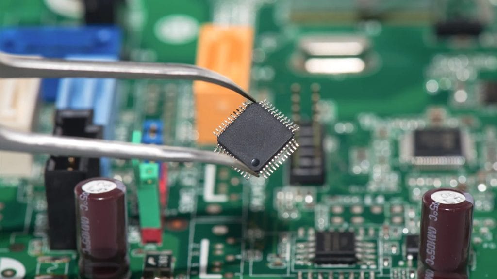
SMT stands for Surface Mounted Technology, and it is the most popular technology and process in the electronics assembly industry. It is a kind of surface assembly technology to place SMC/SMD components and mounted on the surface of pcb (Printed Circuit Board,some where also call PWB)PCB) or the surface of other substrates.
Under normal circumstances, Most of the electronic products we are using were are designed with various capacitors, resistors and other electronic components, thus it needs so a variety of smt chip processing techniques to accomplish this task.

SMT basic process
Solder paste printing –> parts placement –> reflow soldering –> AOI optical inspection –> maintenance –> sub-board.
With the fast development of Electronic, components need to be made more and more miniaturization to compliance with current technology. , and the previously used perforated though hole components can no longer be full filled. Electronic products have more complete functions, and the integrated circuits (ICs) used no longer have perforated components, especially large-scale, highly integrated ICs, which have to use surface mount components. With mass production of products and automation of production, factories must produce high-quality products with low cost and high output to meet customers’ needs and strengthen market competitiveness.
The advantages of smt chip processing: high assembly density, small size and light weight of electronic products. The volume and weight of chip components are only about 1/10 of that of traditional plug-in/through hole components. Generally, after SMT is adopted, the volume of electronic products is reduced by 40%~60 %, the weight is reduced by 60%~80%. High reliability and strong anti-vibration ability. The defect rate of SMT solder joints is low, Good high frequency characteristics, and reducing electromagnetic and radio frequency interference. It is easy to realize automation and improve production efficiency, cost effective, energy saving etc.
It is precisely because of the complexity of the process, there are many professional smt assembly factories around the world. Auspi is among of them, which located in Shenzhen.
The SMT basic process element includes: screen printing (or dispensing), placement (curing), reflow soldering, cleaning, inspection/QA, and repair
- Silk screen: Its function is to print solder paste or patch glue onto the PCB pads to prepare for the soldering of components.
- Dispensing: It is to drop the glue onto the fixed position of the PCB boardbuya glue dispenser.
- Mounting: Mountingcomponents to the fixed position of the PCB by SMT equipment, or it is called Pick and Place Machine.
- Curing/Reflow soldering: Meltingthe patch glue or solder by a reflow oven, so that the surface assembly components and the PCB board are firmly bonded together.
- Cleaning: Its function is to remove the solder residues such as flux that are harmful to the human body on the assembled PCB board. The equipment used is a washing machine, and the location may not be fixed, it may be online or offline.
- Inspection: Inspect the welding and assembly quality of the assembled PCB board. The equipment used includes magnifying glass, microscope, online tester (ICT), flying probe tester, automatic optical inspection (AOI), X-RAY inspection system, functional tester, etc.
- Rework


